Designing and unifying massively interconnected systems: How hard can it really be?
In recent years, there have been significant advancements in hardware acceleration for zero-knowledge proofs (ZKPs). Despite this progress…
Designing and unifying massively interconnected systems: How hard can it really be?
Apr 21, 2023
In recent years, there have been significant advancements in hardware acceleration for zero-knowledge proofs (ZKPs). Despite this progress, achieving widespread adoption of ZKPs still requires significantly higher performance. For example, even with the ZPrize GPU champion, generating a proof with an extended_k value of 28 on Halo2 can still take 50–100 seconds; this is when leveraging a fully populated, top-tier multi-card GPU system. Thus, there is still a need for further optimization to improve the performance of ZKPs and make them more widely accessible.
To achieve near real-time proof generation, we currently face a significant gap of approximately two orders of magnitude. Closing this gap will require the use of massively connected FPGA/GPU/ASIC systems, which must be adopted by all hardware specialists, including ourselves. There are no viable alternatives to this approach at present. Therefore, in production environments, relying on a single FPGA/GPU chip for hardware acceleration is not sufficient. Instead, we all rely on some form of multi-card system to achieve the desired performance.
Some may argue that since MSM is an embarrassingly parallel task, transferring existing designs onto a larger chip or a vast interconnected FPGA system should be relatively straightforward, and intuitively provide us with nice linear scaling properties. Sadly for us all, this is not the case!
Some of the particularities and nuances which lead to great complexity when transitioning from a single-chip system to a massively-connected one, are not yet a focal point for the community discussion surrounding ZK hardware acceleration. However, some industry players, including ourselves, have already explored this approach. For instance, Ulvetanna recently detailed in their blog post “A Throughput-Optimized FPGA Architecture for Goldilocks NTT” that they encountered a 40% PCle bandwidth reduction when testing their multi-card FPGA server with various data chunk sizes. This example highlights the significant obstacles that must be addressed when scaling up and optimizing these systems for improved performance.
As the designer of the SolarMSM system, we would like to share our experiences around designing vast interconnected systems with the community.
A deeper dive into some specifics of the system design: the devil is always in the details!
Power Integrity Problem
Taking the VU13P and VU9P FPGAs as examples, it is important to note that having 1.47x more hardware resources in the VU13P, when comparing it to the VU9P, we do not automatically gain a 1.47x speedup when migrating the design from the VU9P to the VU13P. The first issue that arises in such a transition is power integrity.
FPGA power delivery is not designed to simultaneously support high resource utilization and high frequency. While it is true that the VU13P is larger, the power delivery support does not scale proportionally from the VU9P to the VU13P chip. This means that the power delivery of a standard VU13P is inherently incapable of maintaining both high resource utilization and high frequency. Without special measures to tackle power integrity problem, designs will probably fail to achieve the much anticipated speedup and encounter some wired situations (e.g. interconnect link status unstable) due to the collapse of power integrity. This is just one small example which further illustrates the complexities involved in scaling up FPGA systems.
Signal Integrity Problem
The foundation of a vast interconnected-system is based on its high-bandwidth interconnect. However, it is essential to understand that signal losses occur during transmission due to the laws of physics. The loss of the signal increases as the data rate rises. For instance, a signal bus operating at 32 Gbps can only travel around 4 inches on a typical printed circuit board (PCB) while maintaining an acceptable insertion loss budget. Additionally, the package length of a VU13P chip is roughly 2 inches. These factors demonstrate the difficulties involved in routing high-speed signals, highlighting the daunting challenges in scaling up these systems.
The SolarMSM Gen-1 system boasts an impressive aggregated interconnect bandwidth of >1.2TB/s (>9600Gbps) between FPGA chips. However, the upcoming SolarMSM Gen-2 system yields even more power, with >2.7TB/s (21600Gbps) of interconnect bandwidth between FPGA chips. The increase in performance is staggering, with the new system set to deliver a level of power not seen before.
Feel the power here. We said it would be a Godzilla, not just a lion.
Thermal Problem
The SolarMSM series systems exhibit a similar level of performance per watt when compared to GPU systems. However, even with this high efficiency, achieving the desired level of performance brings about significant thermal challenges. To put this into perspective, a single RTX 3090 GPU consumes 350 watts. Multiplying this power consumption by 10 yields, 3,500 watts, while a 20-fold increase brings it up to 7,000 watts. All of this power must be contained within a single server, which, for reference, is already ten times the power consumption of a standard high-performance PC (800 watts). These figures illustrate the enormous challenge of managing heat dissipation effectively as system performance scales up.
To tackle the significant thermal challenges associated with scaling up performance, we have incorporated a water-cooling system into our design. The SolarMSM Gen-2 system will also feature enhanced thermal capacity, durability, and ease of assembly and disassembly (DFAD). This advanced system ensures more efficient and effective heat management, allowing us to continue improving the system’s performance without compromising its stability or longevity.
Mechanical Problem
PCBs are generally made from a flexible material, which can lead to problems when faced with a poor design. For example, a typical GPU PCB measures 312mm x 112mm and includes power delivery subsystems and thermal design components on board. Without having a sensible mechanical design, this PCB could start bending quite quickly under the weight of all these components.
When a PCB starts to bend, a larger physical gap forms between the hot chips and thermal components, which in turn worsens the thermal load. Additionally, the instability in the physical signal link may cause an automatic signal rate downgrading, further exacerbating the signal integrity problem we spoke about previously. It’s clear that mechanical, thermal and signal integrity issues are all interconnected, and it is of vital importance to address each aspect effectively to ensure the overall stability and performance of the whole system.
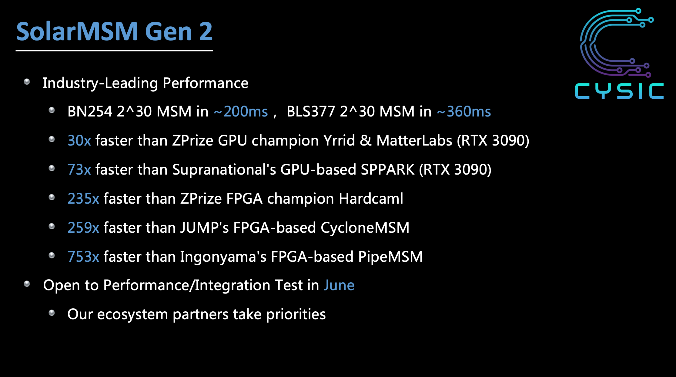
Preview of SolarMSM Gen-2
We are making steady progress on the design of the Gen-2 system. Here’s the preview of the estimated performance.
We would like to thank Luke Pearson for insightful discussions!
Keep exploring Cysic

CyAI: The Decentralized AI Built by Cysic
An open market for verifiable AI inference—moving from trusting a provider to trusting an auditable protocol.

Open-Sourcing Venus: A New Foundation for High-Performance zkVMs
Over the past months, we published a three-part series on how zkVMs should be built, from architectural philosophy to hardware…
zkVM Trilogy (Part III): Building a Production zkEVM Node
Who this post is for: Technical project managers, protocol engineers, and ecosystem participants interested in our concrete execution plan…